In the world of semiconductor manufacturing, precision and accuracy are paramount. Probe cards, an essential component of the semiconductor testing process, play a crucial role in ensuring the functionality and reliability of integrated circuits (ICs). With their intricate design and meticulous manufacturing process, probe cards serve as the vital link between the wafer and the testing equipment. We delve into the fascinating world of Probe Card Manufacturing, exploring the key components, the manufacturing process, and the advancements that have revolutionized this industry.
Understanding Probe Cards:
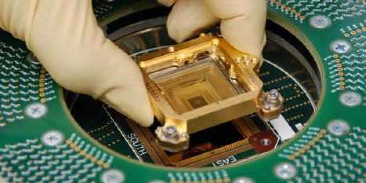
Before diving into the manufacturing process, it is crucial to understand the purpose and composition of probe cards. A probe card acts as a bridge between the wafer, which contains multiple ICs, and the testing equipment. Its primary function is to establish electrical connections with the ICs on the wafer, allowing for the testing of their electrical properties. A probe card consists of several components, including the probe needles, the probe card substrate, and the interconnects.
- Probe Needles
The probe needles, also known as probes or pins, are the most critical component of a probe card. These tiny, needle-like structures make contact with the individual ICs on the wafer, enabling the transfer of electrical signals during testing. The design and construction of the probe needles require meticulous attention to detail. They are typically made of tungsten or beryllium-copper alloys, chosen for their electrical conductivity, durability, and mechanical stability.
- Probe Card Substrate
The probe card substrate serves as the foundation upon which the probe needles are mounted. It provides structural support, electrical connectivity, and thermal management during the testing process. The substrate is usually made of a high-quality ceramic material, such as alumina or silicon. These materials offer excellent electrical insulation and thermal conductivity, ensuring efficient signal transmission and heat dissipation.
- Interconnects
Interconnects are the conductive pathways that facilitate the flow of electrical signals between the probe needles and the testing equipment. They are responsible for transferring the electrical stimuli from the testing equipment to the ICs on the wafer and relaying the responses back for analysis. The interconnects are typically made of gold or other highly conductive metals, ensuring minimal signal loss and impedance.
The Manufacturing Process:
The manufacturing process of probe cards involves several intricate steps that require precision engineering and attention to detail. Let's explore the key stages involved in bringing these essential components to life.
- Design and Prototyping
The manufacturing journey of a probe card begins with the design phase. Skilled engineers, armed with extensive knowledge of electrical engineering and semiconductor testing, develop the probe card's layout, taking into consideration factors such as IC density, contact pitch, and signal integrity requirements. Computer-aided design (CAD) software plays a crucial role in this phase, allowing engineers to create intricate designs and simulate their performance.
Once the design is finalized, the engineers move on to prototyping. Prototyping involves the fabrication of a small batch of probe cards to validate the design and evaluate its performance. This stage allows for adjustments and fine-tuning before proceeding to full-scale production.
- Substrate Fabrication
The next step in the manufacturing process is substrate fabrication. The chosen substrate material, such as alumina or silicon, undergoes precision machining to create the desired shape and dimensions. Specialized tools, such as CNC (Computer Numerical Control) machines, are employed to ensure accuracy and repeatability in the substrate manufacturing process. The substrate may also undergo additional treatments, such as polishing and surface coating, to enhance its electrical and thermal properties.
- Probe Needle Assembly
With the substrate ready, the focus shifts to the assembly of probe needles. This intricate process involves attaching the probe needles to the substrate, aligning them with precision, and securing them firmly. The needles are typically bonded to the substrate using specialized adhesives or welding techniques. It is crucial to ensure proper alignment and uniform contact force across all probe needles to achieve consistent and reliable electrical connections.
- Interconnect Fabrication
Once the probe needles are in place, the interconnects are fabricated. Thin metal films, typically made of gold or other conductive materials, are deposited on the substrate to create the interconnect pathways. This is achieved through various techniques, such as physical vapor deposition (PVD) or sputtering. Careful attention is paid to achieving uniform thickness and adhesion to guarantee optimal electrical performance.
- Testing and Quality Assurance
Quality assurance is of utmost importance in the manufacturing of probe cards. Extensive testing is carried out to ensure the functionality, reliability, and electrical performance of the completed probe cards. Advanced testing equipment is employed to verify the electrical continuity, insulation resistance, and signal integrity of the probe card. Any defective or non-conforming cards are meticulously identified and rectified or discarded to maintain the highest level of quality.
Advancements in Probe Card Manufacturing:
Over the years, the field of probe card manufacturing has witnessed remarkable advancements driven by technological innovations and industry demands. These advancements have played a pivotal role in enhancing the efficiency, accuracy, and performance of probe cards.
- Microfabrication Techniques
Microfabrication techniques have revolutionized probe card manufacturing. With the advent of micro-electromechanical systems (MEMS) technology, it is now possible to fabricate probe cards with ultra-miniature features and intricate designs. MEMS-based probe cards offer higher probe densities, improved alignment accuracy, and enhanced signal integrity, enabling more comprehensive testing of advanced ICs with ever-decreasing dimensions.
- Advanced Materials and Coatings
The availability of advanced materials and coatings has significantly contributed to the performance and longevity of probe cards. For instance, the development of new materials with superior electrical conductivity and mechanical stability has enabled the production of high-performance probe needles. Additionally, the use of specialized coatings, such as low-friction and wear-resistant materials, has extended the lifespan of probe cards, reducing maintenance and replacement costs.
- Multi-DUT (Device Under Test) Capability
To keep pace with the growing complexity of semiconductor devices, probe card manufacturers have introduced multi-DUT capability. This feature allows a single probe card to simultaneously test multiple devices on the wafer, increasing testing throughput and reducing overall manufacturing time. By incorporating advanced circuitry and sophisticated interconnect designs, multi-DUT probe cards have become a game-changer in high-volume production environments.
Conclusion:
Probe cards are the unsung heroes of semiconductor testing, ensuring the quality and reliability of the integrated circuits that power our modern world. The intricate manufacturing process, from design to testing, involves a harmonious blend of engineering expertise, advanced materials, and cutting-edge technologies. As the demand for smaller, faster, and more complex ICs continues to rise, the Probe Card manufacturing industry will continue to push the boundaries of innovation, enabling the semiconductor industry to keep pace with the ever-evolving technological landscape.